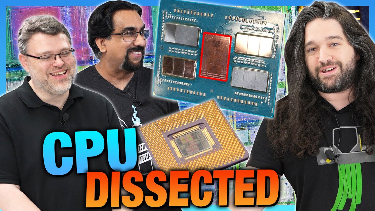
The video offers an in-depth exploration of AMD Ryzen CPU engineering through a detailed analysis of the Threadripper 7995WX die and insights from AMD engineer Amit, highlighting complex aspects like multi-core coordination, cache synchronization, and timing challenges. It also reflects on historical CPU design experiences, inventive problem-solving, and the enduring principles that continue to shape modern processor development.
The video features a detailed discussion about AMD Ryzen CPU engineering, focusing on a deprocessed AMD Threadripper 7995WX die and insights from AMD engineer Amit. The Threadripper die is chemically polished from the back to expose the silicon structures, revealing key components such as the large L3 cache slices, L2 caches per core, and the core engine with floating-point and integer units. Amit explains the chip’s architecture, including the 12 CCDs (core complexes) communicating through the central IO die via a high-speed serial interface called GMI. The discussion highlights the complexity of coordinating multiple cores and cache levels, especially in managing data transfer and synchronization between L3 and L2 caches.
Amit shares his personal contribution to the chip design, focusing on the L3-L2 synchronization block, which handles data transfer between the L3 cache and L2 cache. This block is challenging due to the need to manage voltage level shifting and asynchronous clock domains between the caches, requiring intricate timing and protocol design. Amit explains how timing is critical in CPU design, emphasizing the importance of static timing analysis and simulation to ensure all paths meet frequency requirements. He also touches on the challenge of synchronizing clocks across all cores in a multi-core processor to maintain consistent timing and avoid errors.
The conversation then shifts to an older CPU, the HP PA-RISC 7300LC “Velociraptor” from 1995, which Amit worked on early in his career. This chip had significantly fewer transistors and a simpler design compared to modern Ryzen CPUs but introduced onboard caches and integrated memory controllers. Amit recounts a key challenge involving a critical timing path called the “daddy bus,” which limited the chip’s frequency. He innovated a new circuit to speed up this bus, enabling higher clock speeds and effectively overclocking the chip. The discussion highlights how early CPU design challenges and solutions still influence modern CPU engineering.
An interesting anecdote about lead solder in older CPUs is shared, explaining how radioactive alpha particles emitted from contaminated lead caused random bit flips in cache arrays. This led to a global effort to source low-alpha lead to mitigate these errors. Amit also discusses an unusual signal integrity problem caused by inductive coupling between wires, which was mitigated by placing a metallic gum wrapper on the chip surface to reduce interference—an inventive and unconventional solution. The video also reveals a hidden Easter egg on the Velociraptor chip: a pixel art Velociraptor dinosaur embedded in an unused chip area, demonstrating how engineers sometimes incorporate artwork safely within design constraints.
Finally, Amit reflects on the evolution of CPU design, noting that many fundamental principles from earlier projects still apply today despite increased complexity. He stresses the importance of retaining knowledge and design checks as chip designs scale up in transistor count and frequency. The video closes with stories about the practical challenges in chip manufacturing, such as a mask error that required physically retrieving a mask from the fab to prevent further mistakes. Overall, the discussion provides a rare and insightful glimpse into the intricate engineering, collaborative processes, and creative problem-solving behind modern and historical CPU design.