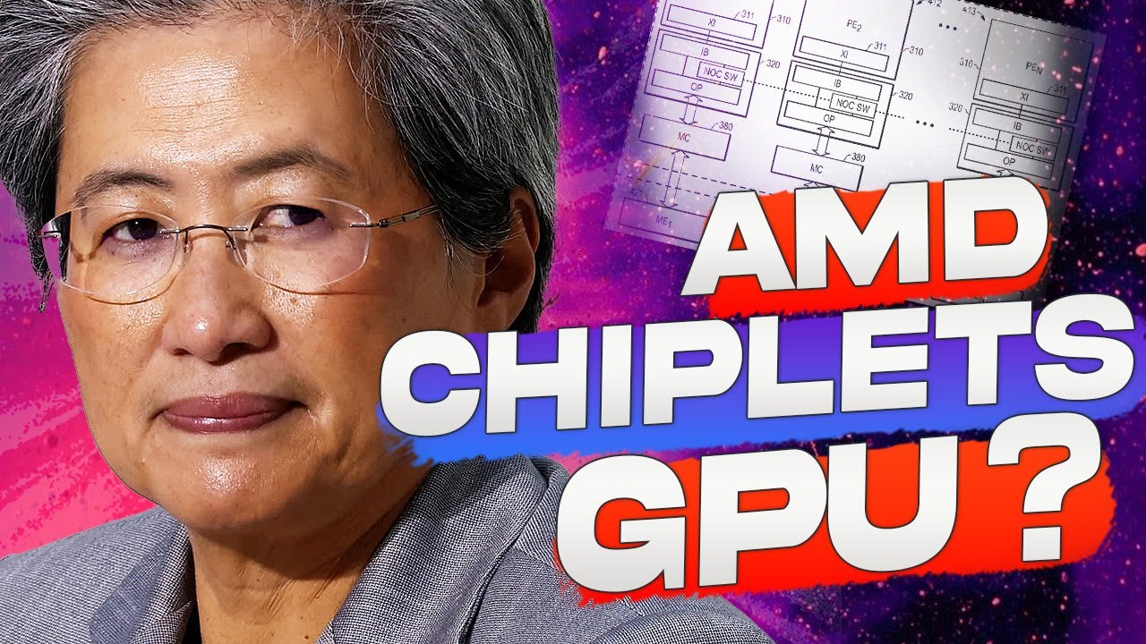
AMD is actively developing chiplet-based gaming GPUs featuring innovations like smart memory management, 3D memory stacking, and thermal solutions to overcome latency, power, and cost challenges, aiming to deliver scalable high-performance GPUs under their unified UDNA architecture. These advancements position AMD to potentially launch disruptive chiplet GPUs that enhance gaming performance and compete strongly against Nvidia in the near future.
The video explores AMD’s ongoing development of chiplet-based GPUs, particularly for gaming applications. AMD has been filing patents that reveal their focus on modular and complex GPU designs, blurring the lines between CPUs and GPUs. One of the significant challenges for chiplet GPUs is managing latency and energy costs stemming from memory access and data movement. AMD’s latest patent introduces a smart switch system that optimizes memory access by deciding whether to migrate tasks or replicate data across chiplets, thereby reducing latency and power consumption. This innovation could allow AMD to create scalable, high-performance GPUs that outperform competitors like Nvidia.
The patent details a system where multiple processing chiplets, each with their own local caches, are connected via a data fabric circuit based on AMD’s Infinity Fabric technology. This setup monitors data locations and schedules tasks to the chiplet that can access the required data most efficiently. By minimizing cross-chiplet data traffic and intelligently managing memory calls, the system aims to keep data and computation close, maximizing throughput and reducing energy use. The design also envisions stacking memory on top of logic dies, similar to AMD’s 3D V-Cache technology, providing both local and shared memory pools for enhanced performance.
In addition to the memory and task management system, AMD is exploring heat management and fabrication cost solutions for 3D stacking through the introduction of bypass chiplets. These dummy dies help transport heat away from the logic chiplets, improving thermal efficiency and potentially lowering manufacturing complexity and cost. This approach makes the prospect of a chiplet-based consumer GPU more realistic, addressing both latency and economic concerns that have traditionally hindered chiplet adoption in gaming GPUs.
AMD’s strategy aligns with their move to unify consumer and data center GPU architectures under the new UDNA (Unified DNA) architecture, which merges RDNA and CDNA. This unification implies that chiplet designs used in data center GPUs will likely translate to consumer gaming GPUs, enabling scalability and shared technology between markets. The video also highlights potential performance improvements in ray tracing with UDNA, suggesting that chiplet architectures could allocate specialized tasks like ray tracing to dedicated chiplets, enhancing parallelism and efficiency through innovations such as wave group threading.
In conclusion, the video argues that AMD is well-positioned to release a chiplet-based gaming GPU, possibly as soon as next year. The combination of patented technologies, architectural unification, and emerging design patterns points toward a future where AMD leverages chiplet modularity and 3D memory stacking to challenge Nvidia’s dominance. While not all patents materialize into products, the evidence suggests that AMD’s chiplet GPU is not only feasible but could be a disruptive force in the GPU market. The video invites viewers to share their thoughts and highlights ongoing technical discussions available to Patreon members.